Methods
I am always open to collaboration, and welcome interested parties to contact me.
Ceramic processing and high-temperature electrochemistry
With a fume hoods, combustion furnace, drying oven, hot plates, mass balance, ball mill, and uniaxial press, we can synthesis ceramics via solid-state or nitrate routes. We also have a thermo-gravimetric analysis setup (TGA) for investigated changes in non-stoichiometry and a dilatometer for studying chemical expansion effects in ceramics.
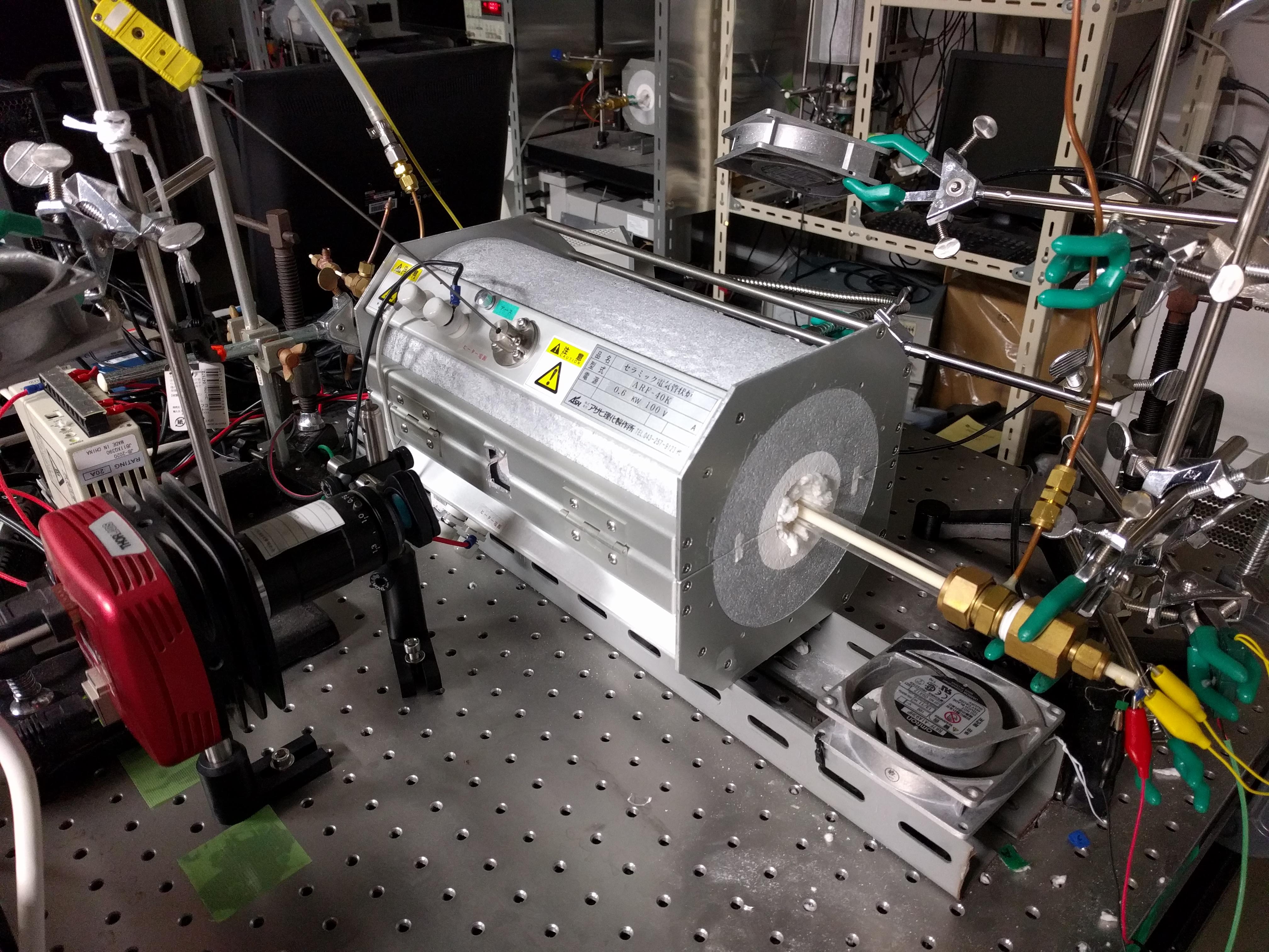
We have several set-up for studying the electrical properties of ceramics and thin films as a function of temperature and oxygen partial pressure. Combined with impedance spectroscopy, this offers a powerful method to separate electrochemical processes with different characteristic time scales and allows the investigation of conductivity, surface exchange rates, and non-stoichiometry, electrically. Furthermore, some of the set-ups have windows for monitoring optical changes in films, which turns out to be a useful tool in investigating the non-stoichiometry and surface exchange in optically active materials. Most of the set-ups can be automated using the LabView software.
Pulsed Laser Deposition (PLD)
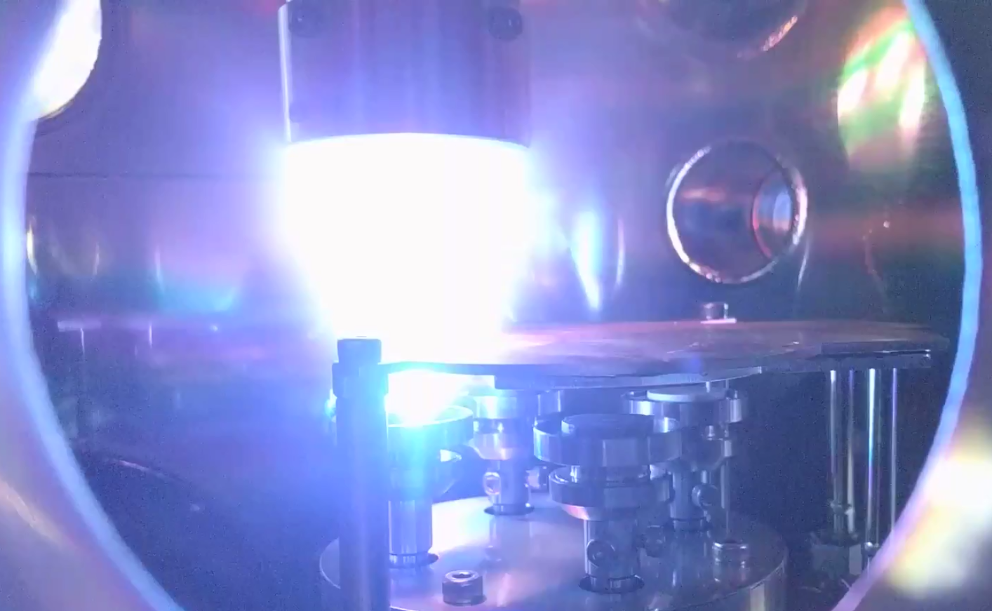
PLD is a technique to grow films of complex oxides easily and routinely (although obtaining the desired composition, orientation, and microstructure is the tricky part). A high energy laser is used to ablate a dense ceramic stoichiometric target to create a ‘plume’ which is incident on a heated (usually single-crystal) substrate. PLD provides a method to fabricate high quality oxide films and a means to control properties such as thickness, strain, crystallinity, grain size and microstructure, as well as engineer well-defined oxide interfaces for study.
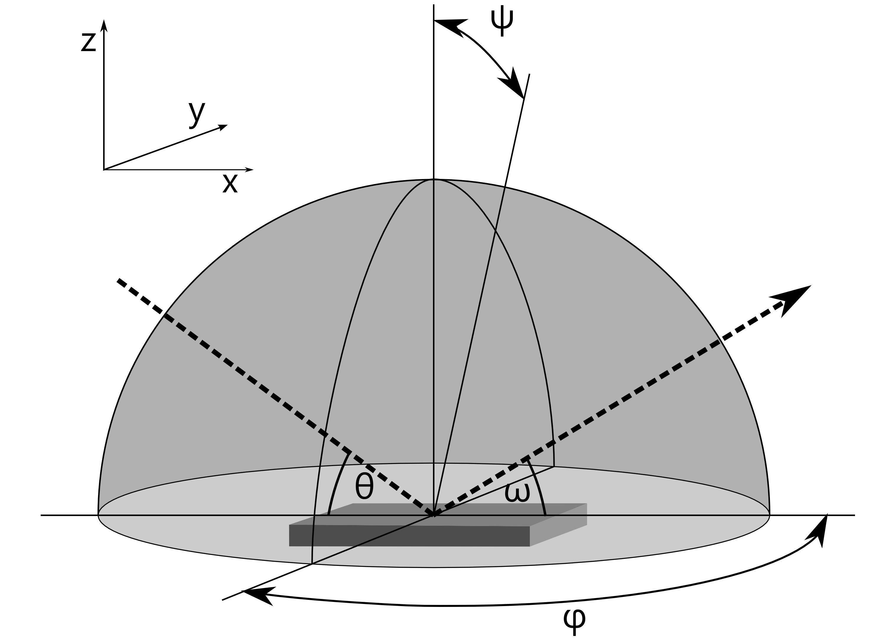
X-ray Diffraction (XRD)
XRD is arguably the most important tool for the characterisation of thin films (along with electron microscopy – see below). It involves scattering a coherent beam of X-rays off the surface region of a sample and detected as a function of scattering angle, and is relatively fast, non-destructive, and highly accurate. XRD can provide information on the thickness, orientation, crystallinity, texture, lattice parameters and strain.
Transmission Electron Microscopy (TEM)
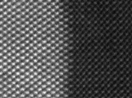
Whereas XRD may be one of the most important tools for thin film engineering, TEM may be one of the most important tools for materials science as a whole. The information provided by TEM complements that obtained from XRD particularly well. While XRD yields information representative of a large proportion of the film volume, TEM probes a much smaller volume, but provides information at sub-atomic spatial resolution.
High energy electrons illuminate a thin cross-section of sample (typically prepared using the ‘lift-out’ method on a dual-beam focused ion beam/scanning electron microscope) producing either a greatly magnified image or electron diffraction pattern. Film morphology, microstructure, orientation relationships, and phase identification, can all be investigated at highly localised regions. Focusing the electron beam to a fine probe and rastering it across the sample (scanning transmission electron microscopy - STEM), opens up powerful new imaging techniques, as well as the ability to gain chemical information at the sub-atomic level with X-ray energy-dispersive spectrometry (XEDS – compositional information) and electron energy loss spectrometry (EELS – composition and electronic structure)./p>
Other facilities/expertise
Also regularly use scanning electron microscopy, Raman spectroscopy, and magnetron sputtering for metal film deposition.
I also have extensive experience in ion beam analysis using low energy ion scattering (LEIS) as well as secondary ion mass spectrometry (SIMS) in conjunction with oxygen isotope tracer diffusion.